公司簡介: A world-class technology company, Advantest is the leading producer of automatic test equipment (ATE) for the semiconductor industry and a premier manufacturer of measuring instruments used in the design and production of electronic instruments and systems. Its leading-edge systems and products are integrated into the most advanced semiconductor production lines in the world. The company also focuses on R&D for emerging markets that benefit from advancements in nanotech and terahertz technologies, and has introduced multi-vision metrology scanning electron microscopes essential to photomask manufacturing, as well as a groundbreaking 3D imaging and analysis tool. Founded in Tokyo in 1954, Advantest established its first subsidiary in 1982, in the USA, and now has subsidiaries worldwide. More information is available at www.advantest.com.
產(chǎn)品推薦


新聞動態(tài)

同是12英寸芯片廠,從打樁到量產(chǎn)粵芯比博世快了2年
據(jù)粵芯半導(dǎo)體官方消息,面對日益增長的終端運用需求,博世已有的6英寸和8英寸芯片工廠不足以滿足自身產(chǎn)品線對芯片的需求,進而把眼光投向于規(guī)模經(jīng)濟更高的12英寸芯片生產(chǎn)線,該

高通:驍龍X55已被全球超過30家廠商采用
10月14日,高通全資子公司高通技術(shù)宣布,驍龍X55 5G調(diào)制解調(diào)器及射頻系統(tǒng)已被全球超過30家OEM廠商采用,以支持商用5G固定無線接入(FWA)CPE終端自2020年開始發(fā)布。與高通合作的OEM廠商

國內(nèi)新布局多座12英寸晶圓廠
日前,聞泰12英寸車規(guī)級功率半導(dǎo)體自動化晶圓制造中心項目宣布簽約落戶上海,該消息備受業(yè)界關(guān)注,國內(nèi)將再添一座12英寸晶圓廠。近年來,隨著國家大力發(fā)展集成電路,國內(nèi)12英寸

總投資10.6億元 上海釜川高端裝備研發(fā)制造項目落地?zé)o錫
近日,江蘇無錫錫山區(qū)東港鎮(zhèn)人民政府與上海釜川自動化設(shè)備有限公司(以下簡稱 上海釜川 )舉行簽約儀式。從洽談到落地僅用20天,總投資10.6億元的釜川高端裝備(半導(dǎo)體、光伏)研

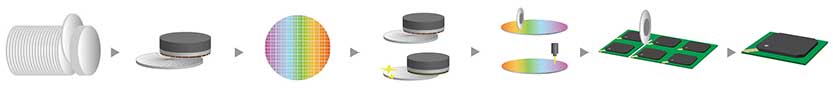
意法半導(dǎo)體制造出首批200mm碳化硅晶圓!
本文《意法半導(dǎo)體制造出首批200mm碳化硅晶圓!》,重點介紹芯片制造/封測細(xì)分領(lǐng)域相關(guān)信息,787字涉及芯片,意法半導(dǎo)體,晶圓制造相關(guān)信息。